I like building stuff with electronics, but for projects expected to actually go into ‘production’, a breadboard just doesn’t cut it. I know I can order PCBs cheap on the internet, but last I checked they’re ether from China and take a while to arrive, or not inexpensive.
So here is the approach I’m currently using to do PCBs at home in a relatively quick and cheap way. Note that ‘beautiful’ is not a word in the previous sentence 🙂 This method is based on ideas and processes I picked up on various sites, particularly https://www.mikrocontroller.net/ has lots of interesting stuff.

I design the PCB in Fusion 360 – I know I can use KiCad but I learned Eagle a few years ago and have a Fusion 360 license for doing 3d printer designs anyway.
Once the PCB is done I select all the relevant bottom layers, and print them in b/w and NOT MIRRORED. The goal is to have an image that is the mirror inverse of what needs to be the etch mask later. This sometimes takes me a few times to get completely right, so I print on normal paper first. The printer must be a laser printer and you need good toner with solid black areas!
Once it looks right I put a piece of magazine paper over it, attached at one end. The paper needs to be the type of slightly glossy, completely smooth thin paper you find in magazines or catalogues. I’m using half a page from an ‘ELV’ catalog here. 🙂 It’s only attached at one end because it needs to go through the laser printer without getting torn or folded and I found this works best on my super cheap Samsung M2020. Be aware that whatever laser printer you use might not like this at all, do at your own risk.

Once I have the size I cut a piece of pure PCB, just copper layer, no photosensitive layer. I find a manual jigsaw works best. After cutting I file off the edges, do a first clean of the surface with steel wool, and then a second clean with acetone to remove all grease from it. (Use gloves!)

I attach the piece of PCB with the copper surface to the printed design, using heat-resistant tape. Then I run it through a laminating machine, any cheap one should do fine. It needs to go through a couple of times, probably based on temperature and size. I just let it run through in all directions until it’s too hot to touch and the paper solidly sticks to the PCB – don’t pull it off!

I cut off most of the paper and soak the whole thing in water for a few minutes. The paper gets ‘darker’ and finally starts showing the underlying PCB layout. At that point I start gently wiping the soaked paper off the board, it should come loose with almost no effort. The toner is left behind, stuck to the copper.
If the toner is not properly sticking to the PCB then the treatment in the laminator was too short or it has not properly soaked. If that happens I clean the PCB with acetone, and go back to the previous step.

In the meantime I’ve preheated the etching solution (just ferric chloride) – the heat bed of a 3d printer works quite well for this 🙂 This will make the etching process take only a few minutes.

Etching in progress. I carefully wobble the PCB around to ensure fresh acid gets to all surface area uniformly. The toner acts as a protective layer, letting the acid remove all of the other copper. Once there is no more shiny copper left I remove the PCB and wash it in water to remove the remaining acid. (Again, use gloves!)
Finally I wipe off the toner with acetone to get the finished PCB. (Did I mention using gloves?)
I occasionally use the same laminating process to also get a silkscreen layer on the other side of the PCB – that’s useful for more complex designs but often unnecessary. I think it should also be possible to do a double sided PCB this way, but most of my designs work well single sided with a couple of jumpers and I avoid the hassle of lining up front and back.

The PCB can be used with the pure copper surface, but I like to put a layer of tin on it to make soldering easier. I found the easiest way is using this “Fittingslötpaste” that’s otherwise used for soldering pipes together. I smear a layer of this stuff on the copper surface, and then heat the whole thing with a heat gun. The paste first looks like its melting, and then it gets solid again. After that I stop applying heat, let it cool, and then wash off the solidified paste with water. Underneath it a uniform layer of tin has covered the copper.
Once all layers are etched/laminated/tinned, it’s time to drill holes as necessary using a drill press. Again I don’t strive for perfection, I just drill everything with an 0.9mm drill and then check if something doesn’t fit.
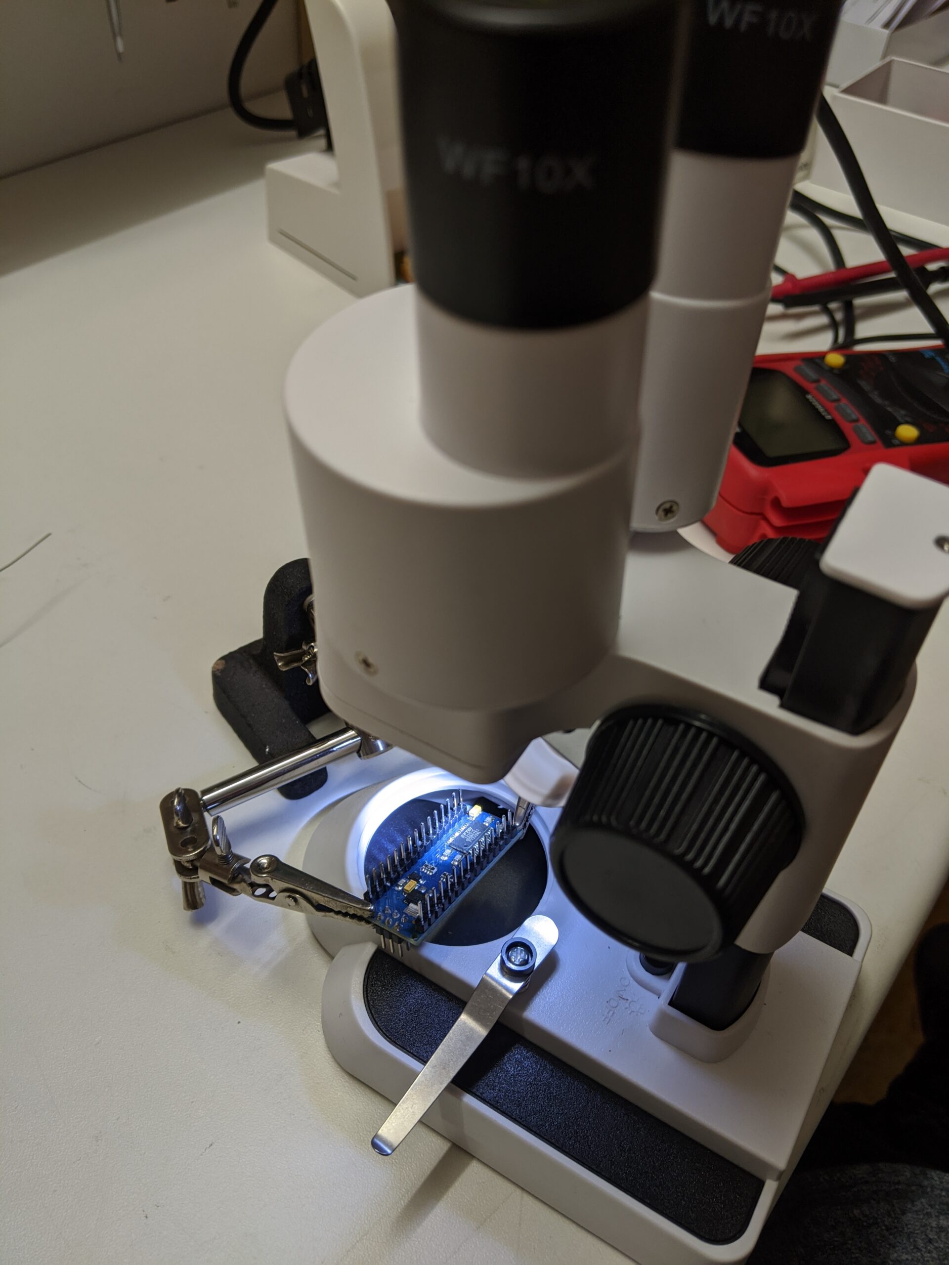
This here is just a simple breakout board for an experiment, but the pinout of the RJ45 connector just doesn’t fit in a breadboard and I didn’t want to order and wait for an alternative.